
Center for Inverse Design
The Center for Inverse Design (CID) was a first-generation (2009–2014) Energy Frontier Research Center funded by the U.S. Department of Energy Office of Science. To address a crucial scientific grand challenge, the Center developed and utilized a new approach to material science. As shown in the figure below, rather than using the conventional direct approach ("Given the structure, find the electronic properties"), we used a "materials by inverse design" approach ("Given the desired property, find the structure").
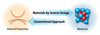
Comparison of the "materials by inverse design" approach (left to right) versus the conventional approach (right to left)
The target properties of interest include general semiconductor optical and electrical properties; the desired materials functionalities include electron- and hole-conductive transparent conductors, solar absorbers, and nanostructures forenergy sustainability. Our predictions of materials are examined iteratively by various synthetic approaches, including high-throughput parallel materials science.
Quick Links

About the Center

Approach

Publications